


US scientists use scanning tunnelling microscopy to reveal the electronic properties of graphene
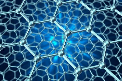
Graphene is a form of carbon with a crystal lattice that resembles a rolled out sheet of hexagonal chicken wire, with a single carbon atom at each vertex of the hexagons. With its unique two dimensional structure and electronic properties chemists believe graphene could be the next big thing in molecular electronics. Now scanning tunnelling microscopy (STM) studies by US scientists have revealed some surprises in the electronic behaviour of this material.1 The findings could help explain graphene's unique behaviour and lead to new ways to build components from this material.
Previously, scientists predicted that graphene's novel nanometre-scale behaviour, such as electronic scattering, spin-based phenomena, and collective excitations, is sensitive to charge-carrier density. To test this Michael Crommie and colleagues at the Lawrence Berkeley National Laboratory and the University of California at Berkeley built a gate-tunable graphene device by attaching nanoscopic gold electrodes to a graphene flake on silicon oxide, mounted on a silicon substrate. With this device and using STM, the team probed the local electronic structure of flakes of graphene while varying the charge-carrier density across the sample.
One particular feature revealed by the team is an unexpected gap in the energy spectrum of electrons tunnelling into graphene's single layer of atoms. This peculiar feature arises because of the interaction of the tunnelling electrons with the vibrations of the two dimensional graphene crystal, the so-called quantised phonons.
'Graphene is a new material, with new physics that could lead to new practical devices and applications', says Crommie. 'In that respect it's as promising as carbon nanotubes, but graphene's planar geometry is potentially even more versatile'.
References
- M. Crommie, Nature Phys., 2008, 4, 627.


No comments yet