


The recent development of low cost, user-friendly scanning tunnelling microscopes (STMs) has brought nanoscience experiments into undergraduate laboratories. These provide real insight into atomic and molecular structure, quantum mechanical effects, as well as the central concepts of nanoscience
-
Scanning tunnelling microscopy provides a window into quantum mechanics for undergraduates
Nanoscience is the study of matter and objects that have dimensions around one billionth of a metre (10-9 m = 1 nm), roughly 80,000 times smaller than the width of an average human hair. Less than 60 years ago most scientists never imagined that we would ever be able to 'see' or 'move' individual atoms which are ~0.3 nm in size. However, with the help of a new breed of microscopes - scanning tunnelling microscopes (STMs) - today's scientists are doing just that.
The ability to image and manipulate nanoparticles has led to numerous technological advances over the past 20 years, including the development of novel materials and nanostructures, such as metal and semiconductor nanotubes and nanowires which show great potential for the miniaturisation of electronic components.1 This in turn may lead to smaller, faster and more efficient computers. Nanomaterials are also being used both in chemical and biological sensors,2 resulting in smaller, more portable devices with higher sensitivity and selectivity than older detectors. Nanostructures are also being used for drug delivery and treatments for tumours.3
Advent of the STM
The scanning tunnelling microscope (STM) was invented in 1981 by Gerd Binnig and Heinrich Rohrer, for which they received the Nobel prize in physics in 1986.4 The STM operates by scanning a very sharp metal tip over the surface of a sample and generating an image. Unlike conventional microscopes, STM does not rely on using visible light to image the sample so its resolution is not limited by the wavelength of light and can be much higher than optical microscopes.
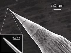
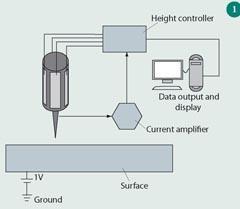
Figure 1 outlines the basic principle of the STM. An atomically sharp, conductive tip, usually made of platinum/iridium or tungsten wire, is brought within a nanometre (10-9 m) of a conductive surface. A voltage is then applied between the tip and the surface. This voltage makes electrons jump from the tip to the surface or, in quantum mechanical terms, they tunnel from the tip to the surface. The result is a small electrical current, the tunnelling current. The STM is capable of detecting very small objects such as atoms because the size of this tunnelling current is exponentially dependent on the distance between the tip and the surface, so that a very small change in distance results in a very large change in tunnelling current. A circuit, the feedback loop, keeps the tunnelling current constant by adjusting this distance, and an image of the surface is generated by plotting the height of the tip as it scans over the surface. The sharpness of the STM tip dictates the quality of the images.
Figure 2 shows a typical STM tip that is sharp even at the nanometre scale. Since the STM image originates from an electrical current, the image contains information about both the topography and the electrical conductance of the sample surface. This also means that any surfaces studied by STM must be electrically conductive for the technique to work.
The STM has been used extensively for investigating surfaces in detail and for manipulating single atoms and molecules. In 1990, Don Eigler and Erhard Schweizer performed a now famous experiment with an STM in which they used the tip to position 35 individual xenon atoms on a nickel metal surface to spell out their corporate logo, IBM.5
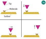
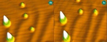
Figure 3 shows an experiment done in our laboratory in which we repositioned individual water molecules on a gold surface. Figure 3(a) shows a schematic of how the STM tip can be used to move individual atoms or molecules. First, the tip is lowered over the atom or molecule to be moved. The tip is moved across the surface, dragging the atom or molecule with it, and then retracted to leave the molecule in its new position. Figure 3 (b) and (c) show individual water molecules on a gold surface before and after manipulation. The two larger lumps on the left of each image are clusters of many water molecules.
STMs for teaching labs
Although most of the major advances have been made on extremely expensive research microscopes, many companies are now marketing a new breed of scanning probe microscopes that are inexpensive and easy to use, and suitable for use in the undergraduate teaching laboratories. STM is a powerful teaching aid because it provides hands-on activities and a visual approach to teaching some of the abstract concepts of quantum mechanics. We find that this enhances students' motivation, understanding and retention of what can be quite difficult topics. Relevant topics that can be addressed by STM experiments include: atomic structure, electron density, particle in a box, electron tunnelling, molecular orbitals and molecular self-assembly. Eigler and his colleagues at IBM, for example, used STM to show how electrons trapped inside different shapes on a surface exhibit quantisation as predicted by the particle in a box theory.6 By choosing the appropriate model systems and surfaces you can design experiments that not only teach students the fundamentals of quantum mechanics as applied to STM, but also introduce important concepts of nanoscience.
Atomic structure experiments
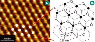
Graphite is an ideal surface for undergraduates to study because it is simple to prepare and easy to scan.7 Removing the top layer from highly oriented pyrolytic graphite (HOPG) with sticky tape yields an atomically flat surface that can be atomically resolved, even with an inexpensive scope. Figure 4 (a) shows an image of HOPG acquired with a teaching STM instrument, recorded with a tunnelling current of 2 nA and a tip voltage of 50 mV. Owing to the symmetry of the graphite surface, all of the atoms are not equivalent and the STM images only every other atom on the graphite surface.8 Figure 4 (b) shows the hexagonal structure of the graphite surface (solid lines) in which every carbon atom is bonded to three others in the same plane, and weakly to the sheet below (dashed lines). The schematic shows that there are two ways in which an atom can be coordinated on the surface of the HOPG - with or without an atom directly below it in the second layer. Because these atoms have different local bonding environments their electron density will vary, and images produced by the STM will be different. Simple, short experiments such as this can introduce concepts including atomic structure, electron density and the interpretation of STM data to undergraduates.
Other surfaces on which atomic resolution can be easily obtained in the teaching lab include titanium, tantalum and molybdenum disulfides (TiS2, TaS2, MoS2).9 Studying these materials allows students to visualise electronic and packing structures of complex materials at the nanoscale.
Molecular resolution
Self-assembled monolayers (SAMs) on a gold surface are also excellent teaching systems that can be used to introduce students to the concepts of molecular assembly. SAMs are composed of a head group that attaches strongly to the underlying substrate and an alkyl chain that may contain other functional groups and can range from one to over 30 CH2 units in length. However, for STM imaging purposes SAMs should be ≤ 12 carbons in length.
Sulfur forms a strong covalent bond to gold, and therefore many SAMs based on alkanethiols in which the head group is a sulfur atom are commonly studied.10 Thiol SAMs on gold are easily prepared by soaking a commercially available gold/mica substrate in millimolar solutions of alkanethiols in ethanol for 24 hours.
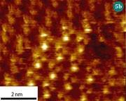
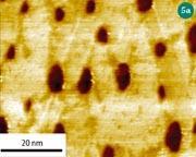
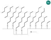
Figure 5(a) is an STM image of an octanethiol SAM (C8 thiol), recorded with a tunnelling current of 0.02 nA and a tip voltage of 1 V. In this image you can see dark holes in the surface, which are 'etch pits'. These are areas where a single layer of gold atoms is missing, but still covered with the SAM. When the C8 thiol molecules bind to the gold surface, some gold atoms are expelled, and etch pits are formed. It is possible to see lines that separate different areas (domains) of the SAM. In each domain the molecules are tilted in the same direction. As the molecules self-assemble on the Au surface their chains are tilted at 30° from the vertical, owing to the van der Waals attraction between their tail groups. Figure 5 (b) is a close-up of the same SAM surface. In this image, you can see the CH3 groups at the end of each alkanethiol molecule. The bright spots are molecular orbitals associated with the methyl groups at the top of each of the molecules. Figure 5 (c) shows the orientation and packing of the SAM layer on the substrate. Such examples also serve to highlight the connection between textbook examples and current advances in nanoscience. Other self-assembled systems that could be studied by undergraduates include monolayers of C60 molecules, surface bound DNA, and carbon nanotubes.9
Details of an undergraduate lab based on SAMs and molecular conductance can be downloaded free from the website.
Mahnaz El-Kouedi is a visiting professor of chemistry from the University of North Carolina at Charlotte; Erin V. Iski is a PhD student and Charles H. Sykes is professor of chemistry in the department of chemistry at Tufts University, Massachusetts 02155-5813, USA.
Acknowledgements
We thank Ashleigh E. Baber and Stephen C. Jensen for their help in the preparation of this article
Related Links
Interactive Nano-visualisation in Science & Engineering Education website
PDF of an article on the STM analysis of highly oriented pyrolytic graphite (HOPG)
Nanosurf
Nanosurf's focus is on the research and development of smart instruments for nanoscience and nanotechnology
STM and single molecule conductance
Lab based at SAMS PDF of article on scanning tunneling microscopy and single molecule conductance by Erin V. Iski, Mahnaz El-Kouedi, and E. Charles H. Sykes at Tufts University
References
- J. Xiang et al, Nature (London), 2006,441, 489.
- S. J. Park, T. A. Taton and C. A. Mirkin, Science, 2002, 295 , 1503.
- J. R. Hirsch et al, PNAS, 2003, 100, 13549.
- G. Binnig et al, Phys. Rev. Lett., 1982, 49, 57.
- D. M. Eigler and E. K. Schweizer, Nature (London), 1990, 344, 524.
- M. F. Crommie, C. P. Lutz and D. M. Eigler, Science, 1993, 262, 218.
- Graphite surface
- H. Holscher et al, Phys. Rev. B, 1998,57, 2477.
- Nanosurfaces
- G. E. Poirier, Chem. Rev., 1997, 97, 1117 .


No comments yet